School of Electrical & Electronic Engineering
DIGITAL ELECTRONICS 1 2010/2011 Session
Lab Assignment Set No 1:
Design of a BCD decoder for a Common Cathode 7-segment LED
A common output device used for displaying decimal numbers is the 7-segment LED display shown in Fig. 1 below. Each of the segments which is labelled with standard letters from a to g, is an LED (or Light Emitting Diode) arranged physically in a matrix such that a decimal digit is displayed when the appropriate segments are lit. For example to display digit two, the LED segments labelled a,b,g,e and d (as illustrated in Fig 1.) must be lit.
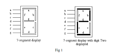
In order to display decimal digits coded in BCD, a BCD-to-7-segment decoder is required as illustrated in fig.2. This device takes BCD inputs and generates at its outputs, the appropriate logic levels for the 7-segment LED display. For example, to display digit ‘2’, the BCD code for decimal 2 which is ‘0010’ must be applied at inputs D C B A of the decoder, with input D being the MSB. The decoder in turn generates the correct logic levels at outputs a, b, c, d, e, f and g so that the correct LED segments are lit to display digit 2.

Your assignment is to do a paper design of this BCD-to-7-segment decoder for a common cathode display using the least possible number of NAND gates (i.e. an optimum design). You are to assume that only BCD numbers are applied to the inputs of the decoder, i.e. you should take advantage of don’t care conditions. Your solutions must show all the design steps taken, i.e. a description of the task, requirements definition, design approaches such as truth-table(s), simplification using K-maps or Boolean theorems, and the implementation (circuit diagrams) using standard logic symbols. Use a Truth-table format as shown below.

On completion of your paper design, you should use NI Multsim and simulate your circuit to verify that your solution works. You are to demonstrate this simulation and submit the simulation file to your Lecturer by Week 12 during your Lab or Tutorial lesson.
Assessment Distribution
Paper Design: 50%
Simulation File: 30%
Demo & Interview: 20 %
____________________________________________________
Truth-table Answer:


School of Electrical & Electronic Engineering
Laboratory Test
Paper Design: 50%
Simulation File: 30%
Demo & Interview: 20 %
____________________________________________________
Truth-table Answer:

K-map answer:

implementation (circuit diagrams) Ans:


Multisims circuit implementation (circuit diagrams) Ans:

download link for multisim circuit implementation
http://www.mediafire.com/?si92mog4v47okk4
____________________________________________________
Laboratory Test
Instructions to Students
1. Read all the instructions and questions carefully.
2. You are expected to work out your solutions on paper before the day of the test. Marks are given for all the preparatory work, accordingly.
3. Bring your Notebook, (installed with NI Multisim), completed test paper and Multisim simulation file with you on the day of the test.
4. You are required to demonstrate your design to your Lecturer in the laboratory according to the instructions given in the test paper.
5. All efforts have been made to ensure that the ICs, the wires and the digital trainer are fully functional. If you believe that an IC or anything else is faulty, inform your Lecturer and it will be replaced.
6. No other help whatsoever will be given to you in getting your circuit working.
There are 7 pages in this Laboratory Test paper.Laboratory Test: A 2-bit Adder Circuit
A two bit Adder is a combinational circuit which is able to add two sets of 2-bit numbers A1 A0 & B1 B0 to produce a sum result which can be up to 3 bits S2 S1 S0. Figure 1 below illustrates.

As an example, the table below shows a typical set of results for input data as given.
Bit 2 | Bit 1 | Bit 0 | Decimal | |
Number A Number B | 11 | 1 | = 3 | |
+ | 1 | 1 | = 3 | |
Sum | 1 | 1 | 0 | = 6 |
Your tasks in this Lab Test is to design, build and test this 2-bit Adder circuit in a number of sequenced steps starting from a simple half adder circuit, progressing to a full adder circuit and finally to a 2-bit Adder. Marks will be given progressively at every stage of the test.
Preparatory Work
The following Sections must be completed before you come for the Laboratory Test |
The ICs given to you for this Lab Test are as follows:
IC Type | Number given |
7408 or 74LS08 | 1 pc |
7432 or 74LS32 | 1 pc |
7486 or 74LS86 | 1 pc |
Section A: Half Adder
A Half Adder adds only two bits A0 and B0 to produce a Sum output S0 and a Carry-out output Cout. Complete the truth table for the Half Adder given below.
Inputs | Outputs | ||
B0 | A0 | S0 | Cout |
0 | 0 | ||
0 | 1 | ||
1 | 0 | ||
1 | 1 | ||
Marks Allocated: | 5 Marks |
Marks Awarded: | / 5 Marks |
From the truth table you have completed, implement the Half Adder circuit using the least possible number of gates and ICs. Draw your circuit in the blank space given below. You are also required to build this circuit and demonstrate its workability to your Lecturer during the Lab Test.

Marks Allocated : | 30 Marks |
Correct Circuit | / 5 marks |
Working Circuit | / 25 marks |
Section B: Full Adder Circuit

Marks Allocated : | 35 Marks |
Correct Circuit | / 5 marks |
Working Circuit | / 30 marks |
Section C: 2 Bit Adder Circuit
The 2-Bit Adder circuit can be constructed using a Half Adder connected to a Full adder as shown in the block diagram below. Using this block diagram, complete the circuit of your 2-bit adder circuit in the blank space provided. Using NI Multisim, capture your completed circuit and save it to your Notebook. In the event that you are unable to get your circuit working on the trainer, you will be required to demonstrate its workability using Multisim to qualify for the marks under “Correct Circuit”. On your test date, construct this circuit on your logic trainer. Hence verify its operation in the presence of your Lecturer by completing the truth table given in the following page. Note that for this circuit, you are required to connect the 2-Bit Adder outputs to one of the 7-Segment digital display on the logic trainer.
Truth Table for verifying correct circuit operation (N.B: To be completed during Test)
Inputs | Outputs | |||
B1 | B0 | A1 | A0 | Digit displayed |
0 | 0 | 0 | 0 | |
0 | 0 | 0 | 1 | |
0 | 0 | 1 | 0 | |
0 | 0 | 1 | 1 | |
0 | 1 | 0 | 0 | |
0 | 1 | 0 | 1 | |
0 | 1 | 1 | 0 | |
0 | 1 | 1 | 1 | |
1 | 0 | 0 | 0 | |
1 | 0 | 0 | 1 | |
1 | 0 | 1 | 0 | |
1 | 0 | 1 | 1 | |
1 | 1 | 0 | 0 | |
1 | 1 | 0 | 1 | |
1 | 1 | 1 | 0 | |
1 | 1 | 1 | 1 | |
Full Adder Circuit Answer:

2 Bit Adder Circuit Answer:

download link for multisim circuit implementation
http://www.mediafire.com/?8b8i50vwfbkwqyv
http://www.mediafire.com/?8b8i50vwfbkwqyv
In order to dealing with a academics pressure, according to study 10% of the people search "make my assignment for me" keyword as students are out of words sometimes. We at Student Assignment Help offers quality solutions with 100% guarantee.
ReplyDeleteGet More Info
ReplyDeleteGet More Info
Get More Info
Get More Info
Get More Info
Get More Info
This post helped me alot. Thanks for sharing with us!
ReplyDeleteFind more about Digital Electronics
You can learn digital electronics from online engineering courses !
ReplyDeleteMy Assignment Help is an incomparable online assignment writing service delivering excellent assignment help service. We have the best in-house team specialist to take complete care of assignment within provided time limit. Convince yourself only after looking at the list of our free samples talking of our quality and expertise
ReplyDeleteI found this is an informative and interesting blog so I think so it is very useful and knowledgeable.
ReplyDeletehoteltowels
bathtowels
hotelsheets
disposableclothing
socks
sokken
socken
kitamiante
hotelfittedsheets
accounts management
ReplyDeleteaccounting package
annual accounts and tax returns
payroll
personal tax returns
accounts management
accounting package
annual accounts and tax returns
payroll
personal tax returns
can i know the password of zip file
ReplyDeleteAn iOS app development course helps learners build high-quality mobile applications. It focuses on real-time development and practical learning. This ios app development course supports professional skill growth. It is dependable.
ReplyDeleteWell written! Our full stack java developer training
ReplyDeleteconnects core concepts with practical development.
Salesforce Administrator Classes
ReplyDeleteVery helpful post, especially for someone new to Salesforce. I came across this salesforce administrator classes recently. Looks like a useful resource.